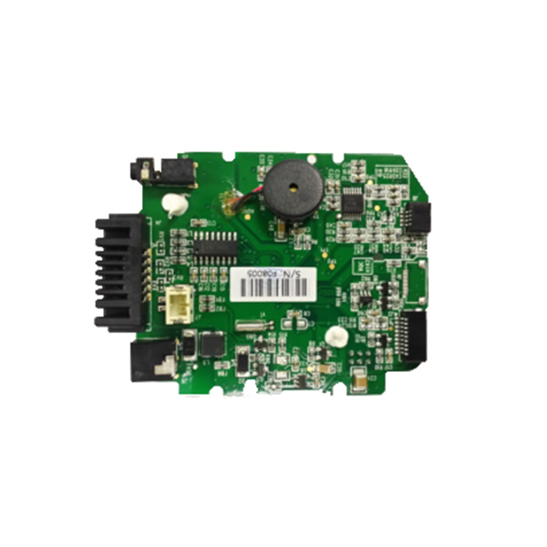
method one:
Print the circuit board diagram on the printer at a ratio of 1:1 on 80 grams of copy paper, find a fax machine, and replace the fax paper with hot melt plastic film. Put the circuit diagram into the entrance of the fax machine, and use the copy button of the fax machine to copy the circuit diagram on the hot-melt plastic film, so that the "manuscript" is done. Use double-sided adhesive tape to flatly paste the plastic film that has been drawn on the copper-clad board, and use a paint brush to evenly brush the paint on the plastic film. After the circuit diagrams are all brushed, remove the plastic film and the printed circuit board is It's printed. After drying, it can be corroded. This method is not a mainstream method, nor can it be mass-produced, as an amateur can try it.

Method Two:
PCB manufacturing printed board map, according to its size, cut the printed board, and clean the copper foil surface. Then, use carbon paper to copy the diagram to the printing plate. According to the actual situation of the component, paste the standard pre-cut symbols of different inner and outer diameters, and then paste the tape lines of different widths depending on the current. Put in ferric chloride for corrosion, take it out and rinse it out in time after corrosion. The next step is to drill the eyes, brighten the copper foil with fine sandpaper, apply rosin alcohol solution, and let it dry.
Method three:
Polish the copper-clad board with fine sandpaper, and then trace the circuit board as required. After the circuit board is drawn, it is corroded in ferric chloride solution. After the circuit board is corroded, use a cotton ball dipped in absolute alcohol to wipe off the protective paint, and dry it before applying pine perfume.
Method four:
Draw up the circuit diagram and cut out the copper-clad board according to its size. Then engrave the circuit diagram on wax paper, cut the wax paper, and place it on the copper-clad board. Take a small amount of paint and talcum powder to make a thin and suitable printing material, dip the printing material with a brush, and evenly apply it to wax paper, repeat it several times, and the circuit can be printed on the printed board.
Then use 1 gram of potassium chlorate and 40 milliliters of 15% hydrochloric acid to prepare a corrosive solution, and apply it to the corroded area on the circuit board for corrosion. After cleaning the circuit board with banana water etc., apply a layer of rosin solution and dry it to drill holes.
